[ad_1]
Jorg Scholvin ’00, MEng ’01, PhD ’06 first set foot in a cleanroom halfway by his undergraduate research. It was the late Nineties and, as a pc science main, he’d registered for a fabrication class for a firsthand have a look at how a pc is assembled. “It’s wonderful to see the way it’s constructed,” he realized, “and to construct it myself.” By the top of the semester, Scholvin had shifted his focus towards electrical engineering and went on to spend a number of years at MIT creating his fabrication abilities.
Now, he guides others by all the chances of the cleanroom as an assistant director at MIT.nano, the Institute’s heart for nanoscale science and engineering.
Initially from Germany, Scholvin has made MIT his residence base for greater than 25 years, minus a short interlude in finance. “Whereas being in a single place, you in the end nonetheless get to expertise very completely different variations of it,” he says of his life on campus as an undergrad, grad scholar, postdoc, and workers member. Since becoming a member of MIT.nano in 2018, the yr it opened, he has helped set up a brand new useful resource for campus analysis: a spot the place all the pieces wanted for nanoscale R&D is positioned underneath one roof. MIT.nano’s instruments are open to the whole MIT group, in addition to exterior customers. However irrespective of the place they arrive from, all those that carry their work by its doorways have entry to professional help from Scholvin and his colleagues.
Exploring the byways
Throughout his undergrad years, Scholvin says, cleanrooms had been primarily a spot for constructing transistors. His doctoral analysis targeted on transistor know-how for top frequency energy purposes, and he collaborated with IBM on new design approaches for such units. Over the previous few many years, researchers at MIT and elsewhere have stretched the boundaries of nanoscale fabrication in lots of different instructions. “The semiconductor trade creates a freeway the place issues are shifting at nice ease and effectivity,” Scholvin says. “Within the tutorial world, you are exploring what’s to the left and the fitting of that freeway. You take all of the little roads and making an attempt to see at what level may that little highway, once more, contribute to this complete development.”
Usually that occurs on the intersections of disciplines. Scholvin skilled that himself throughout his postdoctoral analysis in MIT’s Artificial Neurobiology Group led by Ed Boyden, the Y. Eva Tan Professor in Neurotechnology. Whereas Scholvin developed methods to assemble new sorts of neural recording electrodes, his teammates investigated makes use of for these probes in mind analysis and medication. Collectively, they used Nationwide Institutes of Well being funding to spin the know-how right into a startup — Neural Dynamics Applied sciences.
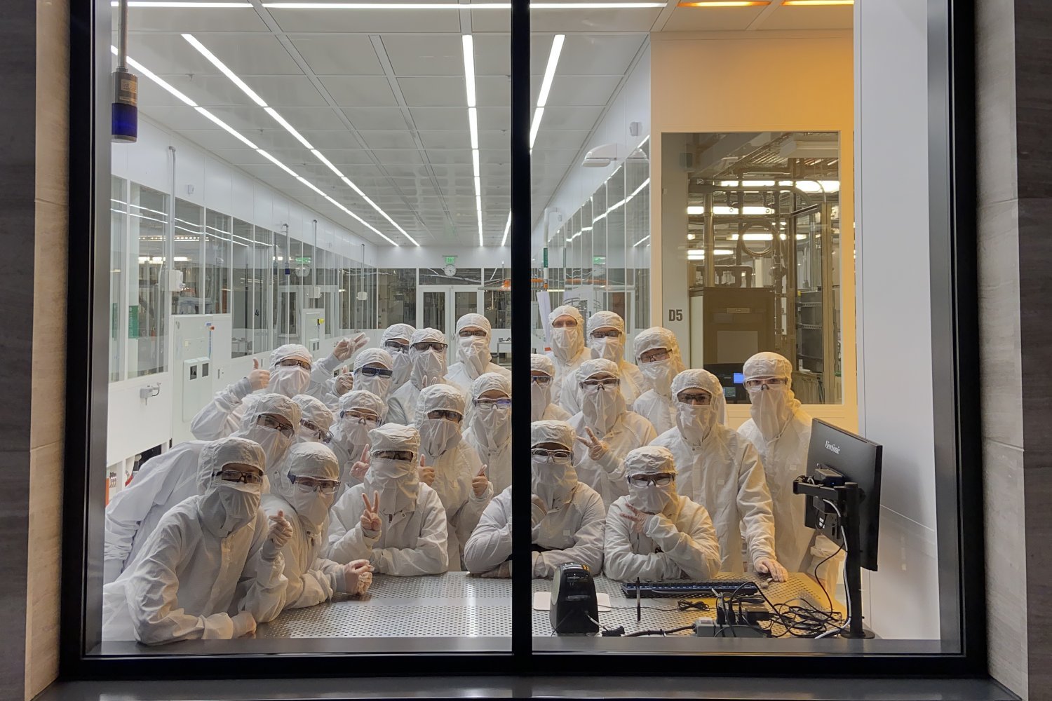
Lately he shares his experience with customers from greater than 50 MIT departments, labs, and facilities, in addition to exterior teams. Scholvin and his fellow instrument specialists seek the advice of with researchers to estimate the time and expense their targets entail, and to establish which among the many 50 or so main fabrication devices at MIT.nano will get the job completed. That suite of instruments (aka Fab.nano) allows the exact engineering of nanoscale constructions and the packaging of these outcomes inside prototype units. Fab.nano’s software set usually overlaps with or enhances instruments for characterization (overseen at MIT.nano by Assistant Director Anna Osherov), which can be utilized to evaluate and analyze the properties of such constructions.
“As director of person providers for Fab.nano, Dr. Jorg Scholvin is tirelessly devoted to serving MIT.nano’s customers, be they undergrads, grads, postdocs, or our trade companions,” says MIT.nano director Vladimir Bulović, the Fariborz Maseeh Professor of Rising Applied sciences. “Jorg isn’t solely educated, however excited to assist.”
The customers who log probably the most hours in Fab.nano areas are those that focus on utilizing new supplies to construct units in areas like electronics and photonics. However Scholvin additionally serves a demographic whose experience lies outdoors fabrication. The most cancers researcher in search of to place a skinny insulating layer on a stainless-steel needle, or the local weather scientist who requires a particular sensor, might not be FAB.nano regulars, “however as a result of they’re ready to make use of our instruments, they will make progress of their different analysis,” he says.
A simple entry level
If Scholvin hadn’t taken that fabrication class as an MIT junior, he may by no means have found his fascination with nature’s smallest constructing blocks. Coming full circle, he now co-teaches a Course 6 lab class to juniors and seniors. However he thinks publicity even earlier within the undergrad expertise may affect extra college students’ trajectories. In fall 2021, he and Donner Professor Jesús del Alamo, his former PhD advisor within the Division of Electrical Engineering and Pc Science, taught a brand new first-year seminar during which eight freshly minted MIT college students had an opportunity to work hands-on within the lab as they discovered the right way to fabricate and take a look at silicon photo voltaic cells.
“Our hope is that these seminars may give college students a straightforward entry level into contributing to analysis,” Scholvin says. “Whilst a first-year scholar, when you’re skilled, you really could make very significant contributions instantly.” He watched his college students’ pleasure develop as they had been challenged first to grasp after which to enhance the processes essential to finish their task. “It definitely is intimidating the primary couple of occasions they’re in there. However as a result of we’re doing the identical steps a number of occasions over, on the finish, they get it they usually’re very comfy.”
“Jorg is a tremendous scientist and educator,” says Dennis Grimard, MIT.nano’s managing director. “He’s captivated with instructing college students to place math and science collectively to resolve issues, and he loves introducing them to MIT.nano. He’d be thrilled to have each single MIT scholar come by one of many labs inside MIT.nano.”
When Scholvin works with college students and meets with MIT.nano guests, he enjoys seeing the second newcomers start to know the true scale of what’s taking place there. “Usually you do not get that appreciation till you really undergo the hidden locations, the services behind the scenes,” he says. “You then understand the sheer massiveness of what is behind it, simply to make the constructing run.”
Serving to to carry MIT.nano from imaginative and prescient into actuality has tapped into that very same ardour Scholvin found as a scholar for determining, layer by layer, the right way to make one thing new. “Whenever you’re becoming a member of an effort that’s already totally developed, you do not get to see the historical past behind these selections,” he displays. “Right here’s an opportunity to drive one thing from the very starting.”
[ad_2]
Source link


